导言
“使用 II-VI 半导体氧化锌 (ZnO) 的光子材料应用正变得越来越普遍,其研究在爆炸式增长,数百个实验室正在研究这种材料的独特特性”[1]。使用 ZnO的一个原因是因为它对环境无害,可作为氮化镓和其他半导体的潜在替代品。另外,它具有生物相容性,非常适合潜在的医疗应用。它在电磁光谱可见部分的波长处是透明的,在紫外波长处是不透明的。此外,它还表现出压电和热电特性。目前,已经为特定的光电应用定制了各种形式的 ZnO,也已使用扫描电子显微镜 (SEM) 中的电子背散射衍射 (EBSD) 表征了其由气相生长过程。
氟化镁 (MgF2)、氧化铝 (Al2O3) 和铝酸镁 (MgAl2O4) 等材料的单晶能够传输红外线 (IR) 和可见光(图 1)。随着纳米结构材料制备的技术进步,现在可以以多晶形式制造这些材料并仍然保持其透过特性。与单晶材料的制造相比,多晶陶瓷材料的制造显著降低了成本。这些多晶陶瓷可以制成高度致密的块状材料,从而减少了孔的形成,减少了孔对透过率的影响。由于这些是陶瓷材料,因此它们具有高强度高硬度,耐损伤且耐热冲击。因此,这些材料非常适合用作防护圆顶和窗户。为了生产具有良好红外透过率的材料,了解影响多晶材料光散射性能的因素非常重要。其一是晶粒尺寸,或更准确地说,是晶界。研究 [2, 3] 表明,减小晶粒尺寸可以提高 MgF2 和氧化铝的透明度。影响透过率的另一因素是组成晶体或织构的择优晶体取向 [4]。 EBSD 是识别此类微观结构特征的理想工具。此外,这些材料的化学组成会影响它们的性能。能谱 (EDS) 非常适合测量微结构内的化学成分及其空间分布,以下部分是这些材料的 EBSD 和 EDS 分析示例。
 图 1. 两个多晶 MgAl2O4 样品显示出不同程度的透明度。
氧化锌(5)
图 2 显示了具有周期性结节的多面 ZnO 微纤维。通过蒸发和沉积工艺制备,可以生产结间距为 5 – 30 µm 的光纤。 可以通过控制生长条件来调节间距。 采用多种技术来表征这些材料,包括 X 射线衍射 (XRD)、EDS 分析、SEM、EBSD 和光致发光 (PL) 显微镜。 特别是,EBSD 可用于表征这些纤维的各向异性生长机制。
 图 2. 具有 6.2 μm 间距的周期性结的 ZnO 微纤维。
图3为一各向异性微纤维生长模型示例。EBSD 测量在几根纤维上证实了这一假定模型。 图 4 中显示了一个示例,使用沿纤维长度制备的 EBSD 进行了取向测量。 从这些取向测量分析中,首先发现纤维确实是单晶。
![Microfiber anisotropic growth model. Through pole figure analysis of the data, it was confirmed that the growth direction of the fibers is <2110>, the “side” surfaces are {0001} planes, and the top and bottom surfaces are {0110} planes. The fiber base was formed by fast growth along the <2110> direction, followed by slow growth along the c-axis [0001] creating the regular prisms.](/-/media/ametekedax/images/resources/application_notes/microstructural_analysis_of_optical_materials/picture3.jpg?revision=9b9c22a9-2ce0-43e0-82aa-dc5022797969&la=zh-cn&hash=4526B6A5907F64452333B41B2F98A361) 图 3. 超细纤维各向异性生长模型。
图 3. 超细纤维各向异性生长模型。
通过对数据的极图分析,确认纤维的生长方向为<2110>,“侧”面为{0001}面,顶面和底面为{0110}面。 纤维基底通过沿 <2110>方向的快速生长形成,随后沿 c 轴 [0001] 缓慢生长,形成规则棱柱。
![EBSD measurements and pole figure analysis. Photoluminescence studies showed that the optical character of the fibers was related to the structure, as can be observed in Figure 5. The photoluminescence behavior means that these modulated fibers could serve as microscale waveguides and make the creation of microscale light-emitting arrays, as well as bar codes used in biotechnology and electronics possible. EBSD has been used to characterize ZnO in other forms and applications. For example, on polycrystalline ZnO varistors [6] and powder compact specimens [7], single-crystal nanoscrews [8], and tetrapods where each leg of the tetrapod is a single crystal [9].](/-/media/ametekedax/images/resources/application_notes/microstructural_analysis_of_optical_materials/picture4.jpg?revision=9864e730-4ee7-47aa-a972-e7427fc350b6&la=zh-cn&hash=DEFE5F74E48F3665305DE2F4CC43E1ED) 图 4. EBSD 测量和极图分析。
图 4. EBSD 测量和极图分析。
光致发光研究表明,光纤的光学特性与结构有关,如图 5 所示。光致发光行为意味着这些调制光纤可以用作微尺度波导,也可以创建微尺度发光阵列,或条形码,可在生物技术和电子产品中使用。 EBSD 已用于表征其他形式和应用的 ZnO, 例如,在多晶 ZnO 压敏电阻 [6] 和粉末压块样品 [7]、单晶纳米螺钉 [8] 和四足体上,其中,四足体的每条腿都是单晶 [9]。
 图 5. 图 2 所示纤维类型的光致发光显微照片。
氟化镁
氟化镁 (MgF2) 具有四方晶体结构。 Wen 和 Shetty [2] 的研究已经表明,晶粒尺寸会影响多晶 MgF2 的透过率。 图 6 显示了 MgF2 在热压然后在不同温度下退火后的取向图。 使用EBSD获得该取向数据,这些图通常被称为取向成像显微镜 (OIM) 图。 EBSD 特别适合表征这些材料的晶粒尺寸。 这些材料的透光能力使得使用传统光学显微镜获得准确的晶粒尺寸测量变得极具挑战性,此外,光学显微镜没有足够的空间分辨率来分辨较小晶粒尺寸的微观结构。 从这里显示的 OIM 图中可以清楚地看出,较高的退火温度会促进晶粒生长的增加。
![Color-coded orientation maps of polycrystalline MgF2 after a) hot-pressing and after b-e) annealing for one hour at the temperatures indicated. (By permission of the authors [2] and sponsoring agency – Naval Air Warfare Center AD.) Optical transmittance measurements were made at several different wavelengths from the polycrystalline MgF2 samples shown in Figure 6. These results are plotted as a function of grain size in Figure 7.](/-/media/ametekedax/images/resources/application_notes/microstructural_analysis_of_optical_materials/picture6.jpg?revision=87ab702d-3dd4-4753-af2e-c1925ddc0297&la=zh-cn&hash=EBC075E93D202566D967D54DAF65A34F) 图 6. a) 热压和 b-e) 在所示温度下退火一小时后多晶 MgF2 的取向图。 (经作者 [2] 和赞助机构——海军空战中心 AD 许可。)
图 6. a) 热压和 b-e) 在所示温度下退火一小时后多晶 MgF2 的取向图。 (经作者 [2] 和赞助机构——海军空战中心 AD 许可。)
在图 6 中所示的多晶 MgF2 样品的几个不同波长下进行光透射率测量。这些结果在图 7 中显示为晶粒尺寸的函数。
![Optical transmittance of polycrystalline MgF2 as a function of grain size at five different wavelengths. The solid lines are from an analytical approximation [3].](/-/media/ametekedax/images/resources/application_notes/microstructural_analysis_of_optical_materials/picture7.jpg?revision=0886fa6c-576d-4992-b32b-61bdd3bc43b4&la=zh-cn&hash=D53668B92507E9A864264B53C232C02A) 图 7. 多晶 MgF2 在五种不同波长下的光透射率与晶粒尺寸的关系。 实线来自解析近似值 [3]。
图 7. 多晶 MgF2 在五种不同波长下的光透射率与晶粒尺寸的关系。 实线来自解析近似值 [3]。
铝酸镁尖晶石
传统上,尖晶石一词指的是红色宝石,但在现代科学文献中,它更具体地指的是镁铝氧化物 (MgAl2O4) 的晶体,有时是指具有特定化学组分和立方晶体结构的一类矿物。 MgAl2O4 晶体在很宽的波长范围内都是透明的。 透射电子显微镜 (TEM) 中的 EDS 已被用于研究细晶尖晶石中跨晶界的化学成分变化的影响 [10]。 图 8 显示了 MgAl2O4 在热压和随后退火后的微观结构。 该图是根据样品上的 EBSD 扫描数据构建的。 图中晶粒的颜色对应于它们相对于样品法线的晶体取向。 其叠加的灰度图是通过将 OIM 扫描中每个点的相应衍射花样的质量对应到灰度来创建的。
![Orientation map overlaid on an intensity map based on EBSD pattern quality on a hot-pressed MgAl2O4 sample. Analysis of the EBSD data obtained for this sample showed very little preferred orientation of the constituent crystals and that the misorientation at the grain boundaries was random. Ting and Lu [11] have studied the role of grain boundaries and sub-grain boundaries on the evolution of microstructure in these materials using selected area diffraction in the TEM. EBSD is an ideal tool for expanding the study of grain boundaries in these materials as it can analyze many boundaries relatively easily, allowing for statistical analysis of grain boundary misorientation [12].](/-/media/ametekedax/images/resources/application_notes/microstructural_analysis_of_optical_materials/picture8.jpg?revision=556c2c81-f43d-4c68-8b19-d05a7b83bc61&la=zh-cn&hash=DB8108BFB0C1BE062BC83A29A67DF447) 图 8. 在热压 MgAl2O4 样品上基于 EBSD 花样质量的灰度图上叠加的取向图。
图 8. 在热压 MgAl2O4 样品上基于 EBSD 花样质量的灰度图上叠加的取向图。
对该样品获得的 EBSD 数据的分析表明,组成晶体的择优取向非常少,并且晶界处的取向差是随机的。 Ting 和 Lu [11] 使用 TEM 中的选区电子衍射研究了晶界和亚晶界对这些材料微观结构演变的作用。 EBSD 是扩展这些材料中晶界研究的理想工具,因为它可以相对容易地分析大量晶界,从而可以对晶界取向差进行统计分析 [12]。
图 9 显示了两个 EDS 图谱,一个对应于热压样品,另一个对应于图 7 中所示的热压和退火样品。谱线显示退火后 Mg/O 和 Al/O 的比率降低。
 图 9. 热压 MgAl2O4 样品和热压退火样品的 EDS 谱。
氧化铝
有趣的是,织构在陶瓷材料的透过性中起着重要作用[4]。 通常,热压粉末压块不会表现出太多织构,因为成型过程往往是各向同性的。 然而,在这些材料中可以观察到一些织构。 例如,图 10 显示了热压透明氧化铝样品的微观结构,并以反极图显示其相应织构。 反极图显示特定晶轴与特定样品取向(在本例中为样品法线)一致。 该材料的平均晶粒尺寸约为 300 nm。 扫描区域包含 1650 个单独的颗粒。 这个数量提供了织构分析的统计准确性[13]。 织构相对较弱; c 轴与样本法线取向一致,其最高强度几乎是随机取向的两倍。
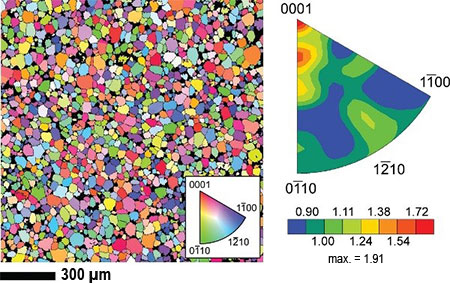 图 10. 热压 Al2O3 样品的取向图和相应织构。
结论
在光学材料领域有几个新的令人兴奋的研究领域,包括开发新材料和现有材料系统的新形式。 了解这些材料中微结构的发展及其在光电性能中的作用对于改进其制造、性能以及将其应用扩展到新的技术领域非常重要。 EBSD 和 EDS 表征微观结构不同方面的能力使其成为将微观结构与特性联系起来的重要工具。
参考文献
- L Savage (2010). Making electro-optical sense with Zinc Oxide” Photonics Spectra 44(2): 47-49
- T.-C. Wen and D. K. Shetty (2009). Birefringence and grain-size effects on optical transmittance of polycrystalline magnesium fluoride.” Proceedings of the SPIE - Window and Dome Technologies and Materials XI, 7302: 73020Z-1- 73020Z-6
- R. Apetz and M. P. B. van Bruggen (2003). “Transparent Alumina: A Light-Scattering Model.” Journal of the American Ceramic Society, 86: 480-486.
- C. S. Chang and M.-H. Hon (2003). “Texture effect of hot-pressed magnesium fluoride on optical transmittance” Materials Chemistry and Physics 81: 27-32
- L. Huang, S. Wright, S. Yang, D. Shen, B. Gu and Y. Du (2004). ZnO well-faceted fibers with periodic junctions”” Journal of Physical Chemistry B 108: 19,901-19,903
- C. Leach (2005). ““Grain boundary structures in zinc oxide varistors”.” Acta Materialia 53: 237-245
- Y. J. Kim, D.-W. Kim, S. J. Ahn, H. S. Kim and S. Ahn (2003). ““Study on the non-linear property of abnormally grown grain ZnO”.” Materials Chemistry and Physics 82: 410-413
- L. Liao, J. C. Li, D. H. Liu, C. Liu, D. F. Wang, W.Z. Song and Q. Fu (2005) “Self-assembly of aligned ZnO nanoscrews: growth, configuration and field emission.” Applied Physics Letters, 86: 083106-1-083106-2.
- B.-B. Wang, J.-J. Xie, Q, Yuan and Y.-P. Zhao (2008) “Growth mechanism and joint structure of ZnO tetrapods.” Journal of Physics D, 41: 102005-1-102005-6
- N. Nuns, F. Béclin and J. Crampon (2005). “Space charge characterization by EDS microanalysis in spinel MgAl2O4.”
Journal of the European Ceramic Society, 25: 2809-2811
- C.-J. Ting and H.-Y Lu (1999) “Hot-Pressing of Magnesium Aluminate Spinel – II. Microstructure Development.” Acta Materialia, 47: 831-840
- V. Randle (2004). ““Application of electron backscatter diffraction to grain boundary characterisation”.” International Materials Reviews 49: 1-11
- S. I. Wright, M. M. Nowell and J. F. Bingert (2007). ““A Comparison of Textures Measured Using X-Ray and Electron Backscatter Diffraction”.” Metallurgical and Materials Transactions A 38: 1845-1855